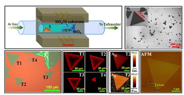
Two-dimensional thin semiconductor materials: single molecule layer or a few molecules of transition metal sulfides, such as molybdenum disulfide (MoS2), tungsten disulfide (WS2) become one of hot topics in the material study due to their unique optical properties, high-performance nanoscale optoelectronic devices and the potential applications of biological molecules and gas detectors. So how to get a large area, high quality, single atomic layer transition metal sulfides single crystal is one of the key issues whether this kind of materials can be put into practical applications.
Our group tried to use chemical vapor deposition method, directly sulfurize tungsten oxide (WO3) with sulfur steam in the inert gas atmosphere. we successfully developed monolayer of WS2 single crystal in triangle shape. The sample was uniform and its size was about 200 microns.
This work is online now at MaterialsViewsChina (MVC), the link is here: http://www.materialsviewschina.com/2014/02/slim-dimensional-semiconductor-material-a-large-area-ws2-monolayer-prepared-and-their-optical-properties-of-single-crystal